

About 2 weeks ago, the PCBs arrived. They look really good and the silkscreen is nice and sharp. Total damage was 24,45€, not including any of the components. I have to say, this already feels a lot more formal than an empty perf board.
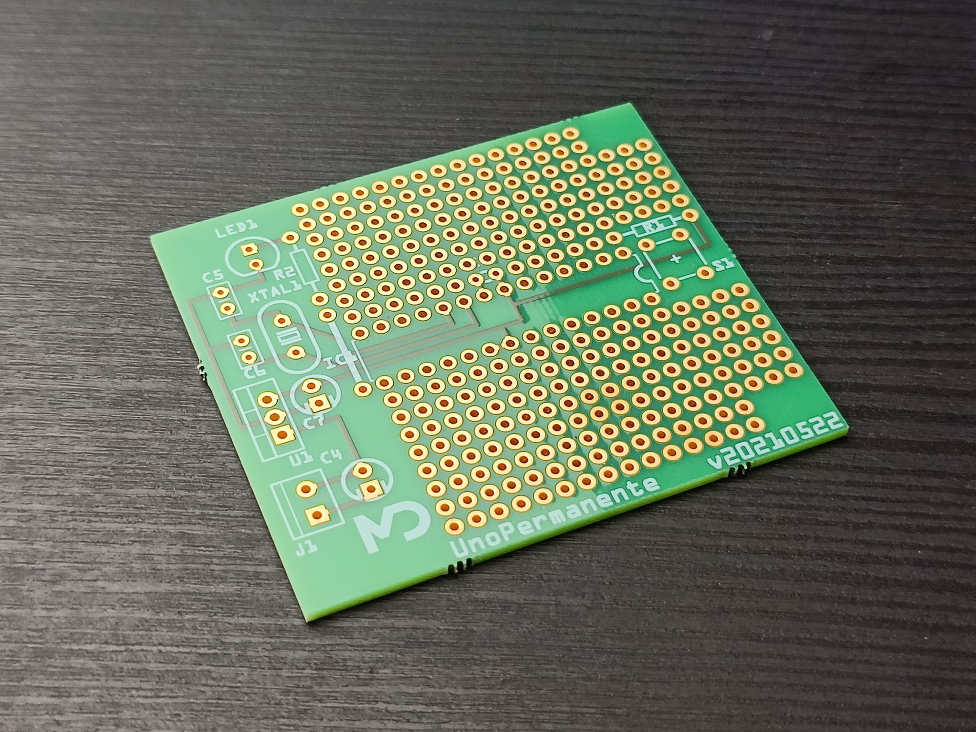
I ordered these PCBs with the full knowledge that I’d make some mistakes and sought to learn from them. So here are the flaws in my design which I aim to fix in the next version:
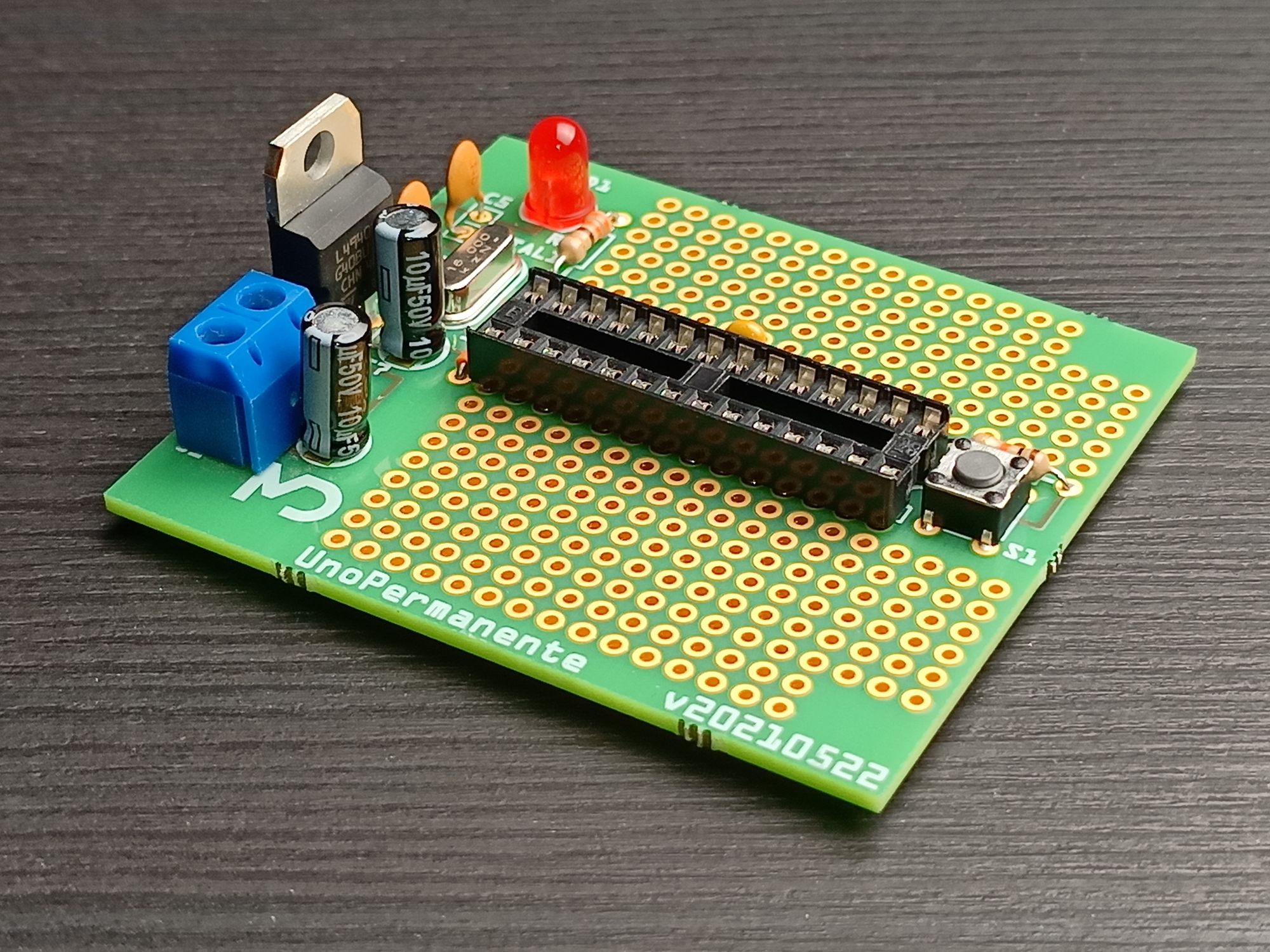
Power supply screw terminal
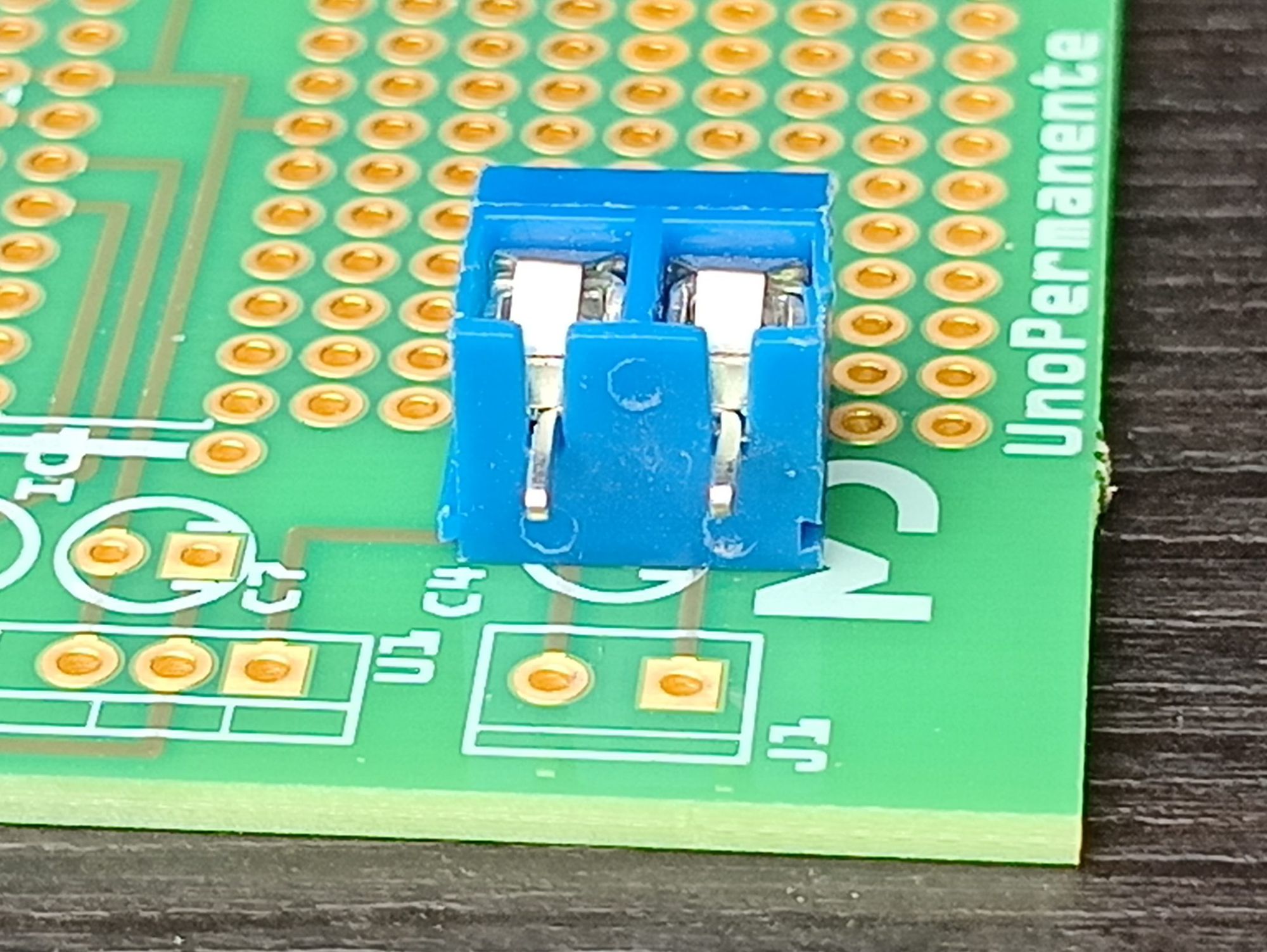 The screw terminal for the power connection had much wider pin spacing than anticipated. Luckily, the pads were large enough to drill an additional hole and then make the connection using a solder bridge.
Incoming ground connection
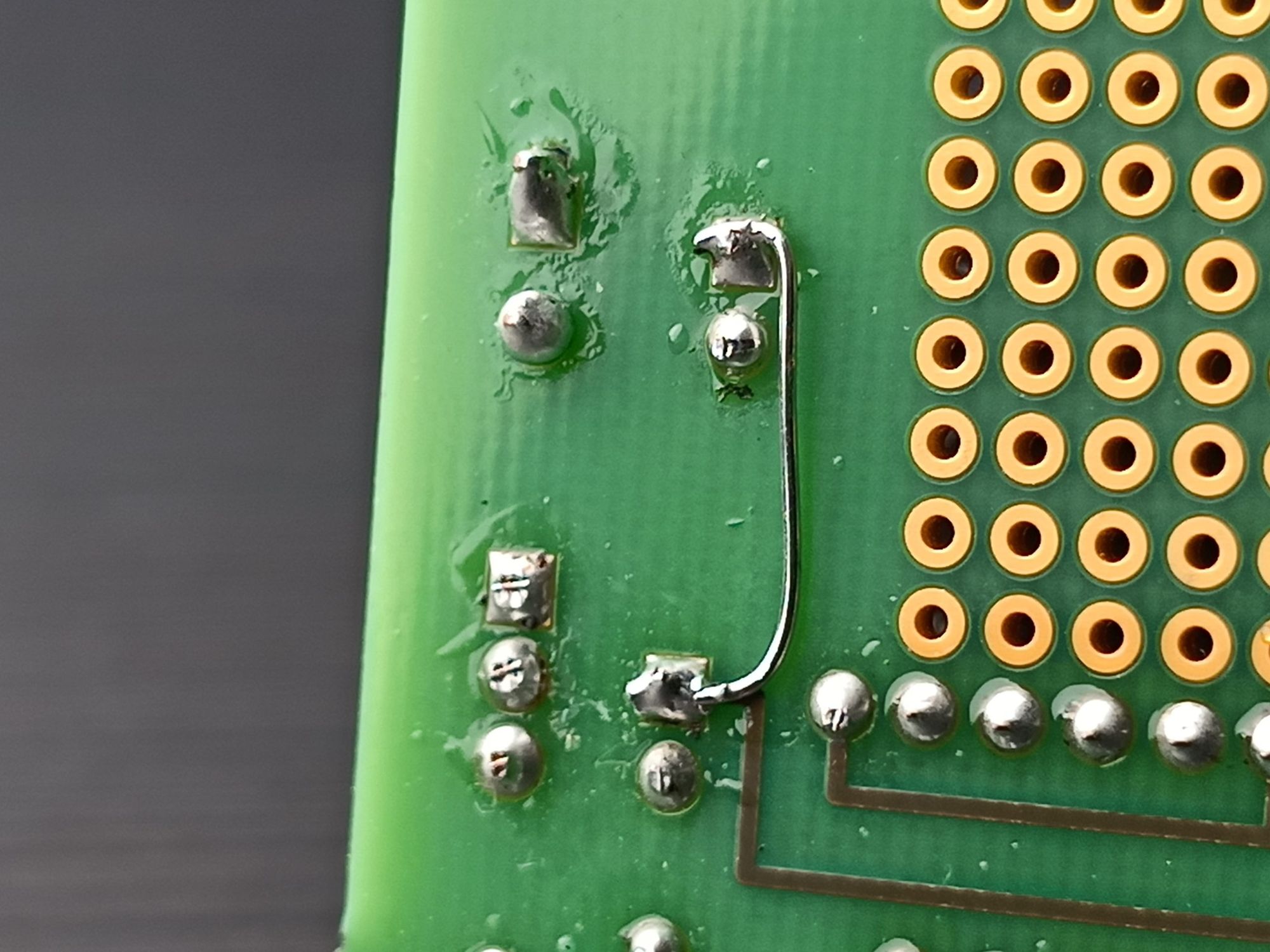 I failed to connect the ground of the incoming power supply to the rest of the circuit, rendering the whole PCB without power. A quite unnecessary mistake as it could have been avoided with a connection trace by hand of the final design. Still easy to fix with a little wire.
In this picture you can also see the hole I had to drill for the screw terminal (top left).
Reset button problems
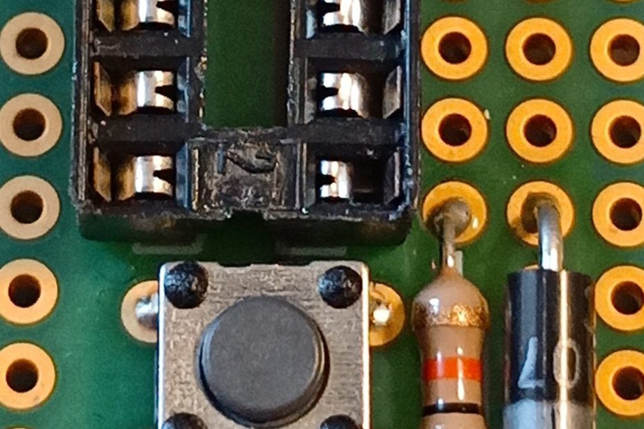 This problem has nothing to do with the PCB but rather the socket for the ATmega that I soldered to it. During my initial testing, the reset button was only working sporadically and I spent quite some time before I figured out the problem: It was the spring contact in the socket. Notice the much larger gap of the last pin on the right compared to the one on the left in the photo. I reused this socket from another project and apparently damaged it when removing it from the old PCB.
It was difficult to track down since, whenever I touched the probe of my multimeter to the pin of the ATmega, I’d push it inwards slightly and it would make contact and work perfectly fine.
No matching enclosure
![]() I honestly thought I designed the PCB around an enclosure, but apparently I didn’t.
I honestly thought I designed the PCB around an enclosure, but apparently I didn’t.
Other than these problems, I could easily populate the PCB with the components. When I was soldering I already got the feeling I sought after for this project: Now, when I want to move a circuit to a permanent PCB, I no longer have to tediously solder all the bootstrap components and I could instead focus on the actual circuit I want to build around the ATmega.
Summary
The flaws I described above can be summed up to the following guidelines for future PCB design:
- Measure all components: Using calipers or a ruler, measure the dimensions and pins of all components to confirm the compatibility with the design. This is especially true for components whose footprint is larger than the outermost leads (such as screw terminals).
- Do a full signal trace of the design: Follow all traces and ensure that the signals (such as power or data) are present at the required connection points.
- Print it out: Before submitting a design for production, print it out and lay the components on their respective place. Also cut it out and place it inside the intended enclosure (if applicable).
What's next
Even though there were some flaws in my first design I reckon I could’ve done a lot worse. After fixing the problems, the PCB worked and I’m overall happy with the result. I’m not going to implement a circuit with this batch (even though I have one in mind) since I failed to design it for an enclosure. In my mind, if a circuit is worth soldering for permanent use, it also deserves an enclosure. So I’ve selected an enclosure which I believe provides adequate space for small projects, the Kemo Electronic GEH KS 28. I selected this enclosure because it would allow for a piggyback PCB arrangement. I already have a PCB designed for it, but I’ll save all that for the next post.


